


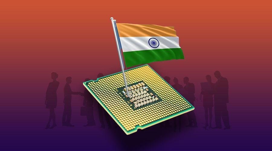
India initiates ambitious plans to establish domestic semiconductor manufacturing capabilities after decades of reliance on imported chips. This strategic pivot aims to secure supply chains, boost local electronics manufacturing, and capture value in the global semiconductor market. xrp price prediction explores the multi-pronged approach India takes toward semiconductor self-sufficiency.
Design expertise creates
India leverages its established semiconductor design capabilities as the foundation for manufacturing ambitions. The country already hosts design centres for numerous global chipmakers, creating complex integrated circuits before sending designs overseas for fabrication.
- Over 2,000 semiconductor patents are filed annually by India-based design teams, demonstrating deep technical expertise
- Design capabilities span from advanced mobile processors to specialised automotive and industrial chips
This design expertise provides critical intellectual property foundations for manufacturing initiatives. Engineers familiar with creating semiconductor designs understand manufacturing requirements and limitations. The existing talent pool means India starts from strength rather than building capabilities from scratch.
Manufacturing incentives
The government introduces substantial financial incentives targeting semiconductor manufacturers. These programs aim to offset the massive capital expenditures required for fabrication facilities while creating favourable operational economics. Production-linked incentive schemes offer manufacturers up to 50% capital expenditure subsidies for facilities built within designated time frames.
The strategy attracts both global semiconductor giants and emerging players seeking manufacturing expansion. Joint ventures between international fabrication leaders and Indian conglomerates create technology transfer mechanisms alongside capital investment. These partnerships accelerate capability development beyond what either domestic or foreign companies could achieve independently.
Specialised technology parks
Purpose-built semiconductor manufacturing zones address infrastructure challenges that previously hindered development. These specialised technology parks provide guaranteed power supply, water treatment facilities, and logistics infrastructure optimised for semiconductor production.
- Uninterrupted power supply systems maintain 99.999% reliability, essential for sensitive fabrication processes
- Water recycling facilities enable 85% water reuse, reducing environmental impact while ensuring an adequate supply
The zones create clustering effects as suppliers, specialised service providers, and downstream electronics manufacturers establish operations nearby. This ecosystem approach addresses challenges beyond chip fabrication, creating complete semiconductor supply chains within geographic proximity.
Talent pipeline expands
- Educational initiatives specifically target semiconductor manufacturing expertise. New specialised programs develop skills across the semiconductor value chain, from materials science to manufacturing process engineering. University partnerships with established global producers create practical training opportunities alongside theoretical education. Scholarship programs specifically target semiconductor-related disciplines to ensure adequate talent pipelines.
- Research grants focus academic attention on manufacturing process improvements and materials innovations relevant to fabrication technologies. These programs extend beyond engineering disciplines, including technician training for the thousands of specialised roles that fabrication facilities require. Technical vocational programs develop skills aligned with industry needs rather than general technical education.
Strategic focus on specific technologies
Rather than attempting to immediately compete across all semiconductor categories, the strategy targets specific technologies aligned with domestic strengths and market opportunities. Power semiconductors, specialised analogue chips, and mature process nodes receive initial focus before expanding to more advanced technologies. This phased approach acknowledges the practical limitations of immediately entering highly competitive segments. By focusing on selected technologies, limited capital and talent resources are concentrated where they create maximum impact. Initial capabilities build foundations for more advanced technologies as the ecosystem matures.
Geopolitical dynamics affect technology transfer arrangements critical for early manufacturing success. Water availability presents particular challenges for water-intensive semiconductor manufacturing processes. Competition from established manufacturing centres in East Asia creates constant cost pressure on new facilities. Despite these challenges, India’s semiconductor strategy represents the most ambitious industrial policy initiative in decades, with implications extending far beyond electronics manufacturing.